For a process controls engineer, hard skills like skill in automation systems, understanding of control theory, and the ability to design and troubleshoot complex processes are important.
Process Controls Engineer Resume Examples & Templates
Looking to showcase your expertise? Our process controls engineer resume examples help you emphasize critical skills like automation, system analysis, and project management that catch employers' attention.

by Gabriela Hernandez, Last Updated: January 18, 2026
Hired By:*

Popular Process Controls Engineer Resume Examples
Discover our top process controls engineer resume examples that demonstrate critical skills such as automation expertise, system optimization, and project management. These samples will help you effectively showcase your professional achievements to potential employers.
Ready to build a standout resume? Our Resume Builder offers user-friendly templates specifically designed for engineering professionals, making the process smooth and efficient.
Recommended
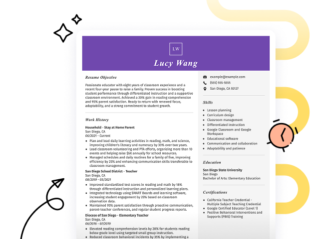
 Customize This Resume
Entry-level process controls engineer resume
What this resume does well:
This entry-level resume for a process controls engineer effectively highlights the applicant's skills in process optimization and automation, showcasing significant achievements like cost savings and efficiency improvements. New professionals must demonstrate their technical competencies and project accomplishments to capture employer interest, especially when faced with limited hands-on experience.
Mid-career process controls engineer resume
What this resume does well:
This resume effectively showcases key qualifications by presenting quantifiable achievements and leadership experience. The structured format highlights the applicant's progression in process controls, demonstrating readiness for advanced responsibilities and complex engineering challenges.
Experienced process controls engineer resume
What this resume does well:
This resume demonstrates the applicant's robust experience as a process controls engineer, highlighting significant achievements such as improving plant efficiency by 15% and reducing operational downtime by 20%. The bullet-point format improves readability, making it easy for hiring managers to identify key accomplishments.
Resume Template—Easy to Copy & Paste
Example
Hiro Zhang
Jacksonville, FL 32203
(555)555-5555
Hiro.Zhang@example.com
Skills
- Process Optimization
- PLC Programming
- SCADA Systems
- HMI Design
- System Integration
- Automation
- Control System Design
- Data Analysis
Languages
- Spanish - Beginner (A1)
- French - Intermediate (B1)
- German - Beginner (A1)
Professional Summary
Dynamic Process Controls Engineer with expertise in optimizing control systems, driving efficiencies, and leading innovative automation solutions to measurable outcomes.
Work History
Process Controls Engineer
Optimal Process Solutions - Jacksonville, FL
January 2024 - October 2025
- Increased efficiency by 15% using PLC systems.
- Reduced costs by ,000 with process optimization.
- Led team to upgrade control systems company-wide.
Automation Specialist
Innovate Automation Inc. - Tampa, FL
January 2022 - December 2023
- Implemented SCADA systems improving uptime by 20%.
- Trained 10 operators in automation safety protocols.
- Saved ,000 annually by optimizing resource use.
Control Systems Engineer
Tech Dynamics - Jacksonville, FL
January 2021 - December 2021
- Integrated HMI solutions for better data access.
- Improved system reliability by 25% with testing.
- Managed installation of new control applications.
Certifications
- Certified Automation Professional - International Society of Automation
- PLC Programmer Certification - Allen Bradley Training Center
Education
Master's Electrical Engineering
University of Texas Austin, TX
May 2020
Bachelor's Control Systems Engineering
Texas A&M University College Station, TX
May 2019
Build Your Resume in Minutes
Creating a custom resume is easier than ever with our Resume Builder!
How to Write a Process Controls Engineer Resume Summary
Your resume summary is the first thing employers will notice, making it important to present a compelling introduction. As a process controls engineer, you should highlight your technical expertise and experience in optimizing systems for efficiency and safety.
This profession involves showcasing skills in automation, control systems, and problem-solving abilities. It's essential to demonstrate how your background aligns with the needs of prospective employers.
To illustrate what a strong resume summary looks like, consider these examples that will help you identify effective strategies and common pitfalls:
Weak Example
I am a process controls engineer with extensive experience in the industry. I am seeking a position where I can apply my skills and contribute to the company's success. A supportive work environment with opportunities for professional development is important to me. I believe that given the chance, I can make a significant impact on your team.
Why this summary misses the mark:
- Includes non-specific statements about skills and experience without concrete examples or achievements
- Overuses personal language which creates filler content instead of focusing on value offered
- Concentrates more on what the applicant desires from the role than what they bring to potential employers
Strong Example
Results-driven process controls engineer with 7 years of experience in the chemical manufacturing industry, specializing in system optimization and automation. Increased production efficiency by 20% through the implementation of advanced control strategies and real-time monitoring systems. Proficient in PLC programming, SCADA systems, and data analysis tools to improve operational performance.
Why this summary works:
- Starts with a clear indication of experience level and industry focus
- Highlights quantifiable achievements that show direct contributions to operational improvements
- Demonstrates relevant technical skills essential for the role, appealing to potential employers
Pro Tip
If you’re new to the field of process controls engineering, consider using a career objective on your resume. This approach can effectively highlight your goals and enthusiasm. There are plenty of tailored resume objective examples available to inspire you.
Showcasing Your Work Experience
The work experience section is the centerpiece of your resume as a process controls engineer. This is where you'll detail the majority of your technical expertise, and effective resume templates always incorporate this important section.
This area should be structured in reverse-chronological order, listing your previous positions. Use bullet points to succinctly highlight your accomplishments and contributions in each engineering role.
Now, let’s look at some examples that will illustrate what a powerful work history looks like for process controls engineers. These examples will clarify what grabs attention and what elements to avoid:
Weak Example
Process Controls Engineer
XYZ Manufacturing Corp – Atlanta, GA
- Monitored control systems.
- Assisted in troubleshooting.
- Collaborated with team members.
- Performed routine maintenance on equipment.
Why this work experience section misses the mark:
- Lacks specific employment dates
- Bullet points are overly vague and do not highlight individual contributions
- Does not include any measurable achievements or outcomes
Strong Example
Process Controls Engineer
TechSystems Inc. – Houston, TX
March 2020 - Present
- Develop and implement advanced control strategies that reduced system downtime by 30%, optimizing production efficiency.
- Lead cross-functional teams to troubleshoot and resolve process issues, achieving a 15% increase in throughput within six months.
- Conduct regular training sessions for staff on new technologies, improving team competency and reducing operational errors by 20%.
Why this work experience section works:
- Starts each bullet with powerful action verbs to convey the applicant’s contributions effectively
- Integrates specific metrics to illustrate the tangible impact of the job seeker's efforts
- Demonstrates relevant technical skills tied to industry standards and practices
While your resume summary and work experience are important components, don’t overlook the importance of other sections that improve your overall presentation. For more detailed guidance on crafting each part effectively, be sure to check our comprehensive guide on how to write a resume.
Top Skills to Include on Your Resume
A well-defined skills section is important for any resume, as it immediately communicates your qualifications to potential employers. It highlights your readiness for the role and helps you stand out in a crowded job market.
For a process controls engineer, focus on technical skills such as skill in PLC programming, knowledge of SCADA systems, and experience with control loop tuning. Including tools like MATLAB and AutoCAD can also effectively showcase your technical capabilities. Soft skills to include are meticulous systems thinking to design and optimize complex automated processes, diplomatic communication to collaborate effectively with operations and IT teams, and the tenacious problem-solving required to troubleshoot intermittent, high-stakes plant failures.
Equally important are soft skills such as problem-solving, communication, and teamwork for collaborating with multidisciplinary teams to optimize system performance and ensure safety compliance.
Selecting the right resume skills is important for meeting employer expectations and ensuring you stand out in a competitive job market. Many organizations use automated screening systems that filter out applicants lacking essential skills, so aligning your qualifications with their needs can make a significant difference.
To effectively highlight your abilities, carefully review job postings related to your desired position. These listings often provide valuable insight into the specific skills recruiters are seeking, helping you tailor your application for both human reviewers and ATS systems.
Pro Tip
Ensure your resume shines and stands out to recruiters. Use our ATS Resume Checker to pinpoint over 30 common errors, helping your application smoothly navigate through applicant tracking systems.
10 skills that appear on successful process controls engineer resumes
Improving your resume with high-demand skills can significantly attract recruiters' attention for process controls engineer positions. You’ll find these essential skills reflected in our resume examples, which empower you to apply confidently.
By the way, consider incorporating relevant skills from this list when they align with your experience and job requirements:
Process optimization
Analytical thinking
Attention to detail
Technical skill
Project management
Team collaboration
Troubleshooting expertise
Data analysis
Regulatory compliance knowledge
Communication skills
Based on analysis of 5,000+ industrial engineering professional resumes from 2023-2024
Resume Format Examples
Selecting the appropriate resume format for a process controls engineer is important as it highlights your technical expertise and relevant project experience, helping potential employers better understand your career journey.
Entry-Level 0 - 2 years
Functional
Focuses on skills rather than previous jobs
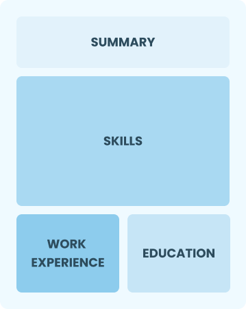
Best for:
Recent graduates and career changers with up to two years of experience
Mid-Career 3 - 7 years
Combination
Balances skills and work history equally
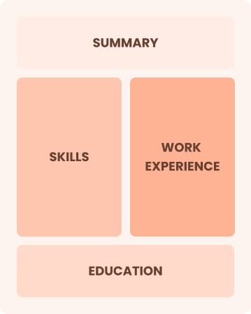
Best for:
Mid-career engineers focused on demonstrating their skills and growth potential
Experienced 8+ years
Chronological
Emphasizes work history in reverse order
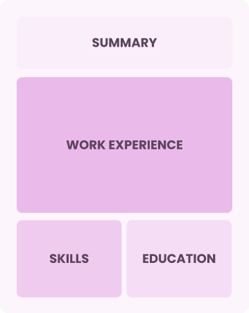
Best for:
Senior engineers excelling in leadership and specialized process controls
Frequently Asked Questions
Should I include a cover letter with my process controls engineer resume?
Absolutely, including a cover letter can significantly improve your application by showcasing your enthusiasm and detailing how your experiences align with the job. It offers a chance to highlight unique qualifications that might not fit into your resume. To get started, explore our comprehensive guide on how to write a cover letter or use our Cover Letter Generator for quick assistance.
Can I use a resume if I’m applying internationally, or do I need a CV?
When applying for jobs outside the U.S., use a CV instead of a resume as it’s often preferred. For guidance on CV formatting and creation, explore how to write a CV for tips on crafting an effective document. Additionally, reviewing CV examples can provide insights that align with international expectations.
What soft skills are important for process controls engineers?
Soft skills such as communication, problem-solving, and teamwork are essential for process controls engineers. These interpersonal skills facilitate collaboration with diverse teams and ensure effective troubleshooting, leading to improved project outcomes and stronger professional relationships.
I’m transitioning from another field. How should I highlight my experience?
Highlight transferable skills like teamwork, analytical thinking, and project management gained from previous roles. These abilities demonstrate your ability to adapt and excel in a process controls engineer position, even without direct experience. Share concrete examples of how you've effectively handled challenges to show your readiness for the responsibilities ahead.
How should I format a cover letter for a process controls engineer job?
To format a cover letter for process controls engineer positions, start by including your contact details, followed by a professional greeting. Craft an engaging opening that links your skills to the role and provides a clear summary of your relevant qualifications. Customizing your content to align with the specific job requirements is key to creating a strong impression.
Should I use a cover letter template?
Using a cover letter template designed for process controls engineers can improve your document's structure and help organize content effectively. This approach ensures you emphasize key skills like automation expertise and project management achievements, creating a strong impression on hiring managers.

Ready to land the job?
Join 28M+ others who've built a resume that works.