


Hard skills are technical abilities like expertise in office software, scheduling, and data management, which contribute to smooth administrative operations.
Administrative Resume Examples & Templates
Looking to stand out in your job search? Our administrative resume examples showcase key skills like organization, communication, and multitasking that help you impress potential employers.

by Gabriela Hernandez, Last Updated: January 18, 2026
Hired By:*

- Popular Administrative Resume Examples
- Resume Template—Easy to Copy & Paste
- Build Your Resume in Minutes
- How to Write an Administrative Resume Summary
- Showcasing Your Work Experience
- Top Skills to Include on Your Resume
- Resume Format Examples
- Administrative Salaries in the Highest-Paid States
- Related Administrative Resume Examples
- Frequently Asked Questions
- Should I include a cover letter with my administrative resume?
- Can I use a resume if I’m applying internationally, or do I need a CV?
- What soft skills are important for administratives?
- I’m transitioning from another field. How should I highlight my experience?
- Where can I find inspiration for writing my cover letter as a administrative?
- How do I write a resume with no experience?
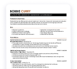
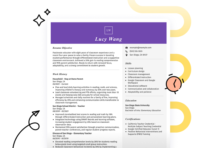
Popular Administrative Resume Examples
Check out our top administrative resume examples that emphasize key skills such as organization, communication, and multitasking. These examples will guide you in showcasing your accomplishments effectively.
Are you ready to build a standout resume? Our Resume Builder offers user-friendly templates specifically designed for professionals in administrative roles, helping you shine in your job applications.
Recommended
 Customize This Resume
Entry-level administrative resume
What this resume does well:
This entry-level resume for an administrative position effectively highlights the applicant's skills in efficiency improvement, client relations, and budget management through quantifiable achievements in previous roles. New professionals must convey their ability to improve operational processes and demonstrate strong organizational capabilities, even with limited direct experience in the field.
Mid-career administrative resume
What this resume does well:
This resume effectively showcases the applicant's qualifications by detailing achievements that emphasize operational efficiency and leadership. The structured presentation of experiences illustrates a clear career progression, demonstrating readiness for more complex administrative challenges.
Experienced administrative resume
What this resume does well:
This work history section demonstrates the applicant's extensive administrative experience, highlighting their ability to improve filing speed by 30% and reduce costs by $5,000. The clear bullet point format allows hiring managers to quickly assess key accomplishments at a glance.
Resume Template—Easy to Copy & Paste
Example
Olivia Davis
Westbrook, ME 04098
(555)555-5555
Olivia.Davis@example.com
Skills
- Office Management
- Scheduling Efficiency
- Document Management
- Communication
- Time Management
- Budget Tracking
- Problem Solving
- Team Leadership
Languages
- Spanish - Beginner (A1)
- French - Intermediate (B1)
- German - Beginner (A1)
Professional Summary
Skilled Administrative professional enhancing efficiency by 30%, experienced in team leadership, office management, and strategic scheduling solutions.
Work History
Administrative
Greenfield Solutions - Westbrook, ME
October 2023 - September 2025
- Managed schedules with 98% accuracy
- Improved filing efficiency by 30%
- Coordinated 40+ weekly meetings
Office Manager
Sunrise Corporation - Westbrook, ME
July 2021 - September 2023
- Streamlined office operations cutting costs by 15%
- Led team of 10 assistants in daily tasks
- Reduced document retrieval time by 20%
Executive Assistant
FutureTech Enterprises - Westbrook, ME
October 2019 - June 2021
- Assisted executives in increasing efficiency by 25%
- Implemented digital scheduling software
- Oversaw expense reports saving ,000 annually
Certifications
- Certified Administrative Professional - International Association of Administrative Professionals
- Project Management Certification - Project Management Institute
Education
Master's Business Administration
University of Illinois Urbana-Champaign, Illinois
May 2018
Bachelor's Management
Illinois State University Normal, Illinois
May 2016
Build Your Resume in Minutes
Creating a custom resume is easier than ever with our Resume Builder!
How to Write an Administrative Resume Summary
Your resume summary is the first opportunity to grab an employer's attention, so it's critical to make a memorable impact. As an administrative professional, you should highlight your organizational skills and ability to streamline processes effectively.
This role demands showcasing your expertise in office management, communication, and multitasking. These qualities are essential in demonstrating how you can contribute to a team's success.
To guide you through crafting an effective summary, here are examples that illustrate what works well and what pitfalls to avoid:
Weak Example
I am an experienced administrative professional with a lot of skills and knowledge. I am seeking a position that allows me to grow and improve my abilities within the company. It is important for me to work in a supportive environment where I can contribute positively to the team. I believe I would be a great addition if given the chance.
Why this summary misses the mark:
- Contains vague phrases like 'a lot of skills' without detailing specific expertise
- Overly focuses on the job seeker's desires rather than highlighting how they can benefit the employer
- Uses generic language that fails to distinguish the job seeker from others in similar roles.
Strong Example
Detail-oriented administrative professional with over 7 years of experience in office management and operations. Streamlined workflow processes that increased department efficiency by 25%, while successfully managing a budget reduction of 15% without compromising service quality. Proficient in Microsoft Office Suite, project management software, and maintaining compliance with regulatory standards.
Why this summary works:
- Begins with specific years of experience and areas of expertise relevant to administration
- Highlights quantifiable achievements that showcase the job seeker's ability to improve efficiency and manage budgets
- Demonstrates technical skills essential for administrative roles, appealing directly to employer needs
Pro Tip
If formal experience isn't in your favor, that's okay! Consider using a career objective to highlight your goals and enthusiasm. There are plenty of resume objective examples tailored for administrative roles that can guide you in crafting a strong statement.
Showcasing Your Work Experience
The work experience section is important for your administrative resume, as it will contain the bulk of your content. Good resume templates consistently emphasize this key area.
This section should be organized in reverse-chronological order, listing your previous positions clearly. Use bullet points to highlight specific achievements and responsibilities that showcase your skills in administration.
To further assist you, we’ll provide a couple of examples that demonstrate effective work history entries for administrative roles. These examples will clarify what works well and what may not be as effective:
Weak Example
Administrative Assistant
XYZ Corp – New York, NY
- Answered phones and took messages
- Scheduled meetings and managed calendars
- Assisted in office tasks and filing
- Interacted with clients as needed
Why this work experience section misses the mark:
- Lacks specific information about job responsibilities
- Bullet points are overly simplistic without showcasing skills or achievements
- Doesn't highlight any measurable outcomes or contributions to the team
Strong Example
Administrative Assistant
Tech Solutions Inc. – San Francisco, CA
March 2020 - Present
- Streamline office operations by developing new filing systems, reducing retrieval time by 30%
- Assist with scheduling and coordinating over 100 meetings monthly, ensuring all logistics are handled efficiently
- Implement a digital inventory tracking system that decreased supply costs by 15% in the first year
Why this work experience section works:
- Starts each bullet with action verbs to clearly convey achievements
- Incorporates specific metrics to demonstrate tangible results from efforts
- Highlights relevant skills such as organization and problem-solving throughout the accomplishments
While your resume summary and work experience are important components, don’t overlook the importance of other sections. Each part of your resume plays a role in showcasing your skills and qualifications. For detailed advice on crafting an effective resume, explore our complete guide on how to write a resume.
Top Skills to Include on Your Resume
A skills section is important for any effective resume because it quickly showcases your qualifications to potential employers. This part of the resume highlights your abilities and can set you apart from other job seekers in a competitive market.
In the administrative field, soft skills are as equally important as soft skills. Where hard skills help you perform the job's unique tasks and goals, soft skills ensure you're efficient and work well with others.
Soft skills, such as strong communication, organization, and problem-solving abilities, help drive collaboration within healthcare teams while improving the overall patient experience.
When selecting skills for your resume, it’s important to align them with what employers expect from job seekers. Many organizations use automated systems to screen out applicants who lack essential resume skills, making this alignment important for getting noticed.
To improve your chances of success, carefully review job postings related to your desired position. This will help you identify key skills that recruiters prioritize and ensure your resume effectively passes through ATS filters.
Pro Tip
Make sure your resume stands out in the digital crowd by using our ATS Resume Checker. It can help you uncover over 30 common errors and boost your chances of passing through applicant tracking systems with ease.
10 skills that appear on successful administrative resumes
Showcasing high-demand skills in your resume is important for attracting recruiters in the administrative field. Highlighting these skills can significantly improve your chances of landing an interview, and you can see them effectively demonstrated in our resume examples.
By the way, if these skills align with your experience and job requirements, consider adding them to your resume:
Communication
Time management
Attention to detail
Problem-solving
Multitasking
Proficient in Microsoft Office Suite
Customer service orientation
Project management
Data entry accuracy
Team collaboration
Based on analysis of 5,000+ administrative professional resumes from 2023-2024
Resume Format Examples
Choosing the right resume format is essential because it highlights your key administrative skills, relevant experience, and career growth in a clear and organized way.
Entry-Level 0 - 2 years
Functional
Focuses on skills rather than previous jobs
Best for:
Recent graduates and career changers with up to two years of experience
Mid-Career 3 - 7 years
Combination
Balances skills and work history equally
Best for:
Mid-career professionals focused on demonstrating their skills and pursuing growth opportunities
Experienced 8+ years
Chronological
Emphasizes work history in reverse order
Best for:
Seasoned leaders driving strategic initiatives in administration
Administrative Salaries in the Highest-Paid States
Our administrative salary data is based on figures from the U.S. Bureau of Labor Statistics (BLS), the authoritative source for employment trends and wage information nationwide.
Whether you're entering the workforce or considering a move to a new city or state, this data can help you gauge what fair compensation looks like for administratives in your desired area.
$0$90K$180K
Frequently Asked Questions
Should I include a cover letter with my administrative resume?
Including a cover letter can significantly improve your application by allowing you to showcase your personality and explain how your skills fit the job. It provides an opportunity to make a personal connection with potential employers. If you need assistance crafting a compelling cover letter, explore our how to write a cover letter guide for easy-to-follow steps. Alternatively, use our Cover Letter Generator for quick results.
Can I use a resume if I’m applying internationally, or do I need a CV?
When applying for jobs abroad, use a CV instead of a resume to provide a comprehensive overview of your academic and professional history. To aid in crafting an effective CV, explore our extensive resources on how to write a CV that offer guidance on formatting. You can also review various CV examples tailored for international standards.
What soft skills are important for administratives?
Soft skills such as communication, problem-solving, and adaptability are essential in administrative roles. These interpersonal skills help foster positive relationships with colleagues and clients, ensuring efficient collaboration and a harmonious work environment.
I’m transitioning from another field. How should I highlight my experience?
Highlight your transferable skills such as communication, organization, and teamwork when applying for administrative roles. These abilities showcase your potential to excel in a new environment, even if you lack direct experience. Provide concrete examples from your past roles that align with key administrative tasks to demonstrate how you can add value to the team.
Where can I find inspiration for writing my cover letter as a administrative?
For those seeking administrative positions, exploring professionally crafted cover letter examples can be incredibly beneficial. These samples provide valuable insights into effective content ideas and formatting strategies, enabling you to present your qualifications clearly and compellingly. Use them as a source of inspiration to improve your application materials.
How do I write a resume with no experience?
If you're applying for administrative positions with limited experience, consider referencing a resume with no experience to help you highlight your organizational skills, skill in software tools, and any internships or volunteer roles. Focus on transferable skills like communication and problem-solving. Employers appreciate enthusiasm and a willingness to learn, so showcase your eagerness to contribute positively to their team.

Ready to land the job?
Join 28M+ others who've built a resume that works.