


Hard skills are technical abilities such as skill in complex equipment, troubleshooting hardware and software issues, and conducting product demonstrations effectively.
Field Application Engineer Resume Examples & Templates
Looking to stand out in your job search? Our field application engineer resume examples showcase technical expertise, problem-solving abilities, and communication skills that employers love.

by Gabriela Hernandez, Last Updated: January 18, 2026
Hired By:*

- Popular Field Application Engineer Resume Examples
- Resume Template—Easy to Copy & Paste
- Build Your Resume in Minutes
- How to Write a Field Application Engineer Resume Summary
- Showcasing Your Work Experience
- Top Skills to Include on Your Resume
- Resume Format Examples
- Related Engineering Resume Examples
- Frequently Asked Questions
- Should I include a cover letter with my field application engineer resume?
- Can I use a resume if I’m applying internationally, or do I need a CV?
- What soft skills are important for field application engineers?
- I’m transitioning from another field. How should I highlight my experience?
- How should I format a cover letter for a field application engineer job?
- How do I add my resume to LinkedIn?
Popular Field Application Engineer Resume Examples
Discover our top field application engineer resume examples that emphasize key skills such as technical expertise, problem-solving abilities, and customer engagement. These examples are designed to help you showcase your accomplishments effectively.
Ready to build your ideal resume? Our Resume Builder offers user-friendly templates tailored for engineering professionals, making the process straightforward and efficient.
Recommended
 Customize This Resume
Entry-level field application engineer resume
What this resume does well:
This entry-level resume for a field application engineer effectively highlights the job seeker's technical skills and achievements, showcasing significant cost savings and client satisfaction improvements from previous roles. New professionals in this field must demonstrate their ability to optimize operations and manage projects through quantifiable results, even with limited experience.
Mid-career field application engineer resume
What this resume does well:
This resume effectively showcases key qualifications by highlighting strong project management and technical support achievements. The strategic presentation of skills and accomplishments signals the job seeker's readiness to tackle advanced challenges and lead initiatives in the field.
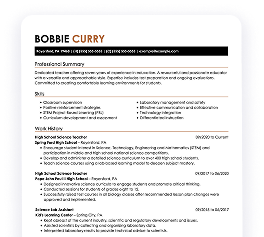
Experienced field application engineer resume
What this resume does well:
This work experience section illustrates the applicant's robust experience as a field application engineer, showcasing achievements like improving system efficiency by 30% and driving 20% annual sales growth. The clear formatting and bullet points significantly improve readability, making it accessible for hiring managers.
Resume Template—Easy to Copy & Paste
Example
Aiko Miller
Chicago, IL 60616
(555)555-5555
Aiko.Miller@example.com
Professional Summary
Field Application Engineer with 8 years in enhancing system processes. Expert in product development, team leadership, and cost reduction strategies driving significant performance improvements.
Work History
Field Application Engineer
TechWave Solutions - Chicago, IL
November 2023 - October 2025
- Mechanically designed systems reducing costs by 20%
- Led team of engineers securing 1.5M in client contracts
- Enhanced technical support process improving satisfaction
Technical Solutions Specialist
InnovateTech Services - Chicago, IL
May 2019 - October 2023
- Implemented strategies boosting sales by 30%
- Coordinated cross-functional teams increasing efficiency
- Developed training programs utilized by 200 professionals
Product Support Engineer
Synergy Technologies - Springfield, IL
May 2017 - April 2019
- Engineered solutions optimizing product performance
- Provided onsite support exceeding client expectations
- Managed documentation processes for 50+ projects
Languages
- Spanish - Beginner (A1)
- German - Beginner (A1)
- French - Beginner (A1)
Skills
- Project Management
- Technical Support
- Client Relations
- Product Development
- Systems Engineering
- Process Improvement
- Team Leadership
- Cost Reduction Strategies
Certifications
- Certified Application Engineer - National Engineering Institute
- Project Management Professional (PMP) - Project Management Institute
Education
Master's in Electrical Engineering Electrical Engineering
University of Texas at Austin Austin, Texas
May 2017
Bachelor's in Electronics Electronics Engineering
California Institute of Technology Pasadena, California
May 2015
Build Your Resume in Minutes
Creating a custom resume is easier than ever with our Resume Builder!
How to Write a Field Application Engineer Resume Summary
Your resume summary is important because it’s the first thing employers see. Make sure it grabs their attention by clearly showing you meet and exceed the job requirements.
As a field application engineer, highlight your technical expertise and ability to solve complex problems. Showcase your experience in providing innovative solutions and excellent customer support.
To better understand what makes a great resume summary, compare these examples. They will guide you on what works well and what doesn’t:
Weak Example
I am a seasoned field application engineer with extensive experience and a record of success. I seek a challenging position where I can use my skills to contribute to the team and achieve personal growth. A company that values innovation and offers career advancement would be perfect for me.
Why this summary misses the mark:
- Lacks specific details about the applicant’s accomplishments or skills, making it too vague
- Focuses on personal desires rather than highlighting what value the job seeker brings to potential employers
- Uses generic phrases that do not differentiate the job seeker from others in similar roles
Strong Example
Results-driven field application engineer with 7+ years of experience in providing technical support and solutions for cutting-edge technology products. Improved customer satisfaction scores by 20% through effective training programs and tailored product demonstrations. Proficient in system integration, troubleshooting, and collaborating with cross-functional teams to drive project success.
Why this summary works:
- Begins with a clear statement of experience level and area of expertise
- Incorporates quantifiable achievement that reflects direct impact on customer satisfaction
- Highlights relevant technical skills and competencies that align with the needs of the engineering industry
Pro Tip
If you’re new to the field or have limited experience, consider using a career objective. This lets you showcase your passion and goals prominently at the top of your resume. For inspiration, explore resume objective examples to help you create your own unique statement.
Showcasing Your Work Experience
The work experience section is important for your resume as a field application engineer, containing the bulk of your content. Good resume templates always emphasize this important part.
This section should list your previous positions in reverse-chronological order, detailing your relevant roles. Use bullet points to highlight specific achievements and contributions you made in each job.
Now, let's look at some examples that illustrate effective work history entries for field application engineers. These examples will clarify what makes an impact and what pitfalls to avoid:
Weak Example
Field Application Engineer
Tech Solutions Inc. – San Francisco, CA
- Provided technical support to clients.
- Assisted with product installations and configurations.
- Collaborated with sales teams for customer needs.
- Conducted training sessions for users.
Why this work experience section misses the mark:
- Lacks specific employment dates to show job duration
- Bullet points do not highlight any measurable achievements or results
- Descriptions focus on routine tasks rather than showcasing expertise or impact
Strong Example
Field Application Engineer
Tech Innovations Inc. – San Francisco, CA
March 2020 - Present
- Provide technical support for product installations, achieving a 95% customer satisfaction rating through effective troubleshooting and training.
- Develop tailored solutions for clients, resulting in a 30% increase in efficiency across multiple projects over the past year.
- Conduct on-site demonstrations and workshops that improve client understanding of products, leading to a 20% boost in sales within six months.
Why this work experience section works:
- Each bullet point starts with an action verb that clearly explains the applicant's contributions
- Includes specific metrics to showcase the impact of the applicant's work on customer satisfaction and business outcomes
- Demonstrates relevant skills such as problem-solving, communication, and technical expertise vital for a Field Application Engineer
While your resume summary and work experience are important components, don't overlook the importance of other sections that contribute to a well-rounded document. For more detailed insights on how to write a resume, be sure to explore our comprehensive guide.
Top Skills to Include on Your Resume
Including a skills section on your resume is important as it provides a snapshot of your capabilities. This helps potential employers quickly assess if you have the qualifications needed for the field application engineer role.
A strong resume shows hiring managers you have the right mix of hard and soft skills.
Soft skills are interpersonal qualities like strong communication, problem-solving, and teamwork that facilitate collaboration with clients and improve customer satisfaction in the field.
When selecting skills for your resume, it’s important to align them with what employers expect. Many organizations rely on automated systems to filter out applicants who lack essential resume skills. This step is key in securing an interview.
To effectively capture the attention of recruiters and pass ATS checks, review job postings carefully. Look for specific skills mentioned and prioritize those that match your experience to improve your chances of standing out.
Pro Tip
Ensure your resume stands out by using our ATS Resume Checker. This tool highlights over 30 common errors, helping you navigate applicant tracking systems with ease and confidence.
10 skills that appear on successful field application engineer resumes
Improve your resume to capture the attention of hiring managers by highlighting essential skills sought for field application engineer roles. You can find these skills illustrated in our resume examples, giving you the confidence to pursue opportunities successfully.
Here are 10 key skills that you should think about including in your resume if they align with your expertise and job criteria:
Problem-solving
Technical skill
Communication
Project management
Customer support
Software troubleshooting
Data analysis
Collaboration
Attention to detail
Adaptability
Based on analysis of 5,000+ engineering professional resumes from 2023-2024
Resume Format Examples
Selecting an appropriate resume format is important for a field application engineer, as it showcases essential technical skills and experiences in a clear, powerful way that reflects your career journey.
Entry-Level 0 - 2 years
Functional
Focuses on skills rather than previous jobs
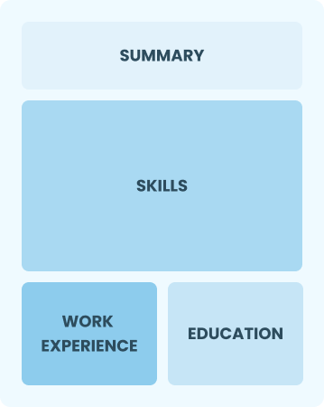
Best for:
Recent graduates and career changers with up to two years of experience
Mid-Career 3 - 7 years
Combination
Balances skills and work history equally
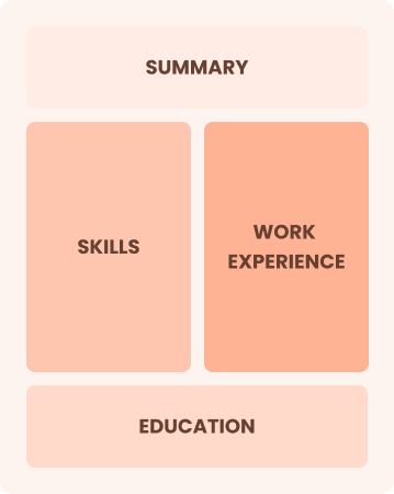
Best for:
Mid-career professionals focused on demonstrating their skills and potential for growth
Experienced 8+ years
Chronological
Emphasizes work history in reverse order
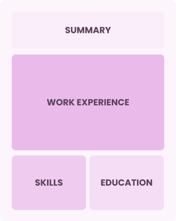
Best for:
Engineers excelling in technical leadership and innovative solutions
Frequently Asked Questions
Should I include a cover letter with my field application engineer resume?
Absolutely. Including a cover letter is essential as it allows you to showcase your personality and enthusiasm for the position. It also provides an opportunity to highlight specific experiences that align with the job requirements. If you need assistance, our guide on how to write a cover letter or our Cover Letter Generator can simplify the process and elevate your application.
Can I use a resume if I’m applying internationally, or do I need a CV?
When applying for jobs outside the U.S., a CV is often required instead of a resume. A CV offers a comprehensive overview of your academic and professional history. Explore our resources on how to write a CV and review CV examples to ensure you present yourself effectively to international employers.
What soft skills are important for field application engineers?
Soft skills like communication, problem-solving, and adaptability are essential for field application engineers. These interpersonal skills facilitate effective collaboration with clients and team members, ensuring that solutions are tailored to meet specific needs while fostering strong professional relationships.
I’m transitioning from another field. How should I highlight my experience?
Highlight your transferable skills such as teamwork, analytical thinking, and communication acquired from previous jobs. These abilities showcase your adaptability and readiness to excel in a field application engineer role. Connect specific examples from your past work to demonstrate how your strengths can meet the demands of this position effectively.
How should I format a cover letter for a field application engineer job?
When you format a cover letter for a field application engineer, begin with your contact information and a professional greeting. Include an engaging introduction, emphasize your technical skills and relevant experience, and show how they align with the job requirements. Wrap up with a compelling call to action that conveys your enthusiasm for the role.
How do I add my resume to LinkedIn?
To add your resume to LinkedIn and improve its visibility, upload it to your profile or highlight your skills and achievements in the "About" and "Experience" sections. This approach helps recruiters in the field find qualified job seekers more easily, increasing your chances of being noticed for opportunities.

Ready to land the job?
Join 28M+ others who've built a resume that works.