


Expertise in hard skills like clinical trial protocols, data management, and regulatory compliance is essential for ensuring accurate and reliable research outcomes.
Clinical Research Associate Resume Examples & Templates
Looking to stand out in your field? Our clinical research associate resume examples showcase expertise in data analysis and trial coordination, helping you capture employers' attention.

by Gabriela Hernandez, Last Updated: January 18, 2026
Hired By:*

- Popular Clinical Research Associate Resume Examples
- Resume Template—Easy to Copy & Paste
- Build Your Resume in Minutes
- How to Write a Clinical Research Associate Resume Summary
- Showcasing Your Work Experience
- Top Skills to Include on Your Resume
- Resume Format Examples
- Related Medical Resume Examples
- Frequently Asked Questions
- Should I include a cover letter with my clinical research associate resume?
- Can I use a resume if I’m applying internationally, or do I need a CV?
- What soft skills are important for clinical research associates?
- I’m transitioning from another field. How should I highlight my experience?
- Where can I find inspiration for writing my cover letter as a clinical research associate?
- How do I add my resume to LinkedIn?
Popular Clinical Research Associate Resume Examples
Check out our top clinical research associate resume examples showcasing key skills like data management, regulatory compliance, and effective communication. These samples demonstrate how to highlight your accomplishments in a way that attracts potential employers.
Ready to build your own impressive resume? Our Resume Builder offers user-friendly templates specifically designed for professionals in the clinical research field, helping you shine in your applications.
Recommended
 Customize This Resume
Entry-level clinical research associate resume
What this resume does well:
This entry-level resume emphasizes the job seeker's strong foundation in clinical trial management and impressive achievements, such as significant improvements in data accuracy and compliance. New professionals in this field should effectively highlight their technical skills and relevant experiences to demonstrate their capability and readiness for a clinical research associate role, even with limited work history.
Mid-career clinical research associate resume
What this resume does well:
This resume effectively showcases qualifications by detailing extensive clinical trial experience and a strong educational background. The clear articulation of responsibilities and accomplishments illustrates readiness for advanced roles, highlighting the applicant's expertise in compliance and data management.
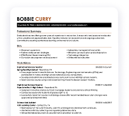
Experienced clinical research associate resume
What this resume does well:
This work experience section demonstrates the applicant's robust experience as a clinical research associate, highlighting their management of 15 trials and a 20% increase in participant recruitment. The use of bullet points improves readability, making it easy for hiring managers to quickly identify key accomplishments.
Resume Template—Easy to Copy & Paste
Example
Aya Miller
Columbus, OH 43204
(555)555-5555
Aya.Miller@example.com
Professional Summary
Experienced Clinical Research Associate skilled in trial coordination, data analysis, and protocol development. Proven track record in streamlining processes and enhancing research efficiency.
Work History
Clinical Research Associate
EverGreen Clinical Services - Columbus, OH
January 2024 - November 2025
- Coordinated 12 investigator meetings yearly
- Monitored clinical data for 30% accuracy lift
- Streamlined trials, cutting costs by 10,000
Research Analyst
BioSolutions Research Group - Cincinnati, OH
April 2021 - January 2024
- Analyzed data for 15 projects monthly
- Implemented database protocols, reducing errors by 40%
- Improved study efficiency, saving 20,000 annually
Clinical Study Assistant
MedTech Innovations - Columbus, OH
March 2018 - March 2021
- Maintained databases, enhancing data entry by 50%
- Facilitated communication for 10 cross-functional teams
- Optimized research processes, cutting costs by 5%
Skills
- Clinical Trial Coordination
- Data Analysis
- Protocol Development
- Regulatory Compliance
- Patient Recruitment
- Time Management
- Risk Assessment
- Project Optimization
Certifications
- Certified Clinical Research Coordinator - SOCRA
- GCP Certification - National Institutes of Health
- Advanced Data Management - ACRP
Education
Master of Science Clinical Research Management
Harvard University Cambridge, MA
June 2018
Bachelor of Science Biology
University of Massachusetts Amherst, MA
June 2016
Languages
- Spanish - Beginner (A1)
- French - Beginner (A1)
- German - Beginner (A1)
Build Your Resume in Minutes
Creating a custom resume is easier than ever with our Resume Builder!
How to Write a Clinical Research Associate Resume Summary
Your resume summary is the first thing employers will see, making it important to create a compelling introduction that showcases your qualifications. As a clinical research associate, you should emphasize your analytical skills, attention to detail, and experience in managing studies.
This profession thrives on showcasing your ability to ensure compliance with regulatory standards and maintain data integrity. Highlighting these core competencies will set you apart in the competitive job market.
To guide you in crafting an effective summary, we’ll present some examples that illustrate what works well and what pitfalls to avoid:
Weak Example
I am a dedicated clinical research associate with extensive experience in various projects. I aim to find a position where I can use my background and contribute positively to the team. A company that values innovation and provides good opportunities for advancement would be perfect for me.
Why this summary misses the mark:
- Lacks specific details about relevant skills or achievements, making it hard to gauge the applicant's qualifications
- Overuses personal pronouns, which detracts from professionalism and focus on employer needs
- Emphasizes what the job seeker seeks from the job rather than highlighting how they can benefit the organization
Strong Example
Detail-oriented clinical research associate with over 6 years of experience in managing multi-site clinical trials, ensuring compliance with regulatory standards and protocols. Successfully improved data accuracy by 20% through implementation of rigorous monitoring processes and training sessions for site staff. Proficient in electronic data capture systems, CRF design, and statistical analysis software to facilitate efficient trial management.
Why this summary works:
- Begins with specific years of experience and job focus, highlighting expertise in clinical trials
- Includes a quantifiable achievement that shows direct impact on data integrity and compliance
- Mentions relevant technical skills essential for the role, demonstrating readiness for the responsibilities
Pro Tip
If you’re new to the field of clinical research, don’t worry if your formal experience is limited. Consider crafting a career objective that highlights your passion and goals. To make a strong impression, refer to these resume objective examples that can guide you effectively.
Showcasing Your Work Experience
The work experience section is the cornerstone of your resume as a clinical research associate. This area will contain the bulk of your content, and effective resume templates always prioritize this section.
It should be laid out in reverse-chronological order, listing your previous positions clearly. Incorporate bullet points to highlight specific achievements and contributions made in each role.
To guide you further, we'll present a couple of examples that illustrate what makes a powerful work history for clinical research associates. These examples will clarify what works well and what may fall short:
Weak Example
Clinical Research Associate
Health Innovations Corp – Boston, MA
- Assisted with clinical trials.
- Maintained study documents.
- Collaborated with research teams.
- Followed protocols and guidelines.
Why this work experience section misses the mark:
- Lacks specific employment dates for context
- Bullet points are vague and do not highlight key skills or achievements
- Emphasizes basic tasks rather than strong contributions or results
Strong Example
Clinical Research Associate
Global Clinical Trials, Inc. – San Diego, CA
March 2020 - Current
- Manage and monitor clinical trial sites to ensure compliance with regulatory standards and protocols, improving site performance by 30%.
- Facilitate investigator meetings and training sessions, resulting in improved understanding of trial objectives among study staff.
- Analyze data and prepare comprehensive reports that contribute to successful regulatory submissions and approvals.
Why this work experience section works:
- Uses strong action verbs to clearly outline the job seeker's contributions
- Incorporates specific metrics to demonstrate the impact of actions taken
- Highlights relevant skills essential for a Clinical Research Associate role through detailed achievements
While your resume summary and work experience are important components, it's important not to overlook other sections that contribute to your overall presentation. For detailed guidance on crafting a standout resume, be sure to check out our comprehensive guide on how to write a resume.
Top Skills to Include on Your Resume
A well-defined skills section is important for a strong resume as it quickly showcases your qualifications to potential employers. It allows you to highlight the specific expertise that makes you a suitable applicant for the role.
Help your resume stand out to employers by combining hard and soft skills.
Meanwhile, soft skills such as strong communication, attention to detail, and problem-solving abilities foster effective collaboration with study teams and improve patient safety throughout the research process.
When selecting your resume skills, it's important to align them with what employers expect from their ideal applicants. Many organizations use automated screening tools to filter out applicants who lack essential skills for the position.
To effectively highlight your qualifications, carefully review job postings for insights on which skills to emphasize. This approach not only grabs the attention of recruiters but also ensures your resume meets the criteria set by ATS systems.
Pro Tip
Elevate your job application success with our ATS Resume Checker. This powerful tool highlights over 30 common mistakes, ensuring your resume stands out and easily navigates applicant tracking systems.
10 skills that appear on successful clinical research associate resumes
Highlighting essential skills on your resume can significantly attract the attention of recruiters looking for clinical research associates. You’ll discover these sought-after skills illustrated in various resume examples, allowing you to approach job applications with a professional advantage.
Here are 10 skills you should consider including in your resume if they fit your qualifications and role requirements:
Attention to detail
Analytical thinking
Effective communication
Problem-solving abilities
Team collaboration
Knowledge of Good Clinical Practices (GCP)
Clinical trial management
Data analysis expertise
Regulatory compliance understanding
Patient recruitment strategies
Based on analysis of 5,000+ medical professional resumes from 2023-2024
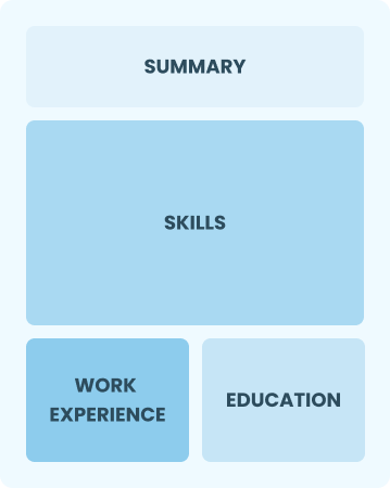
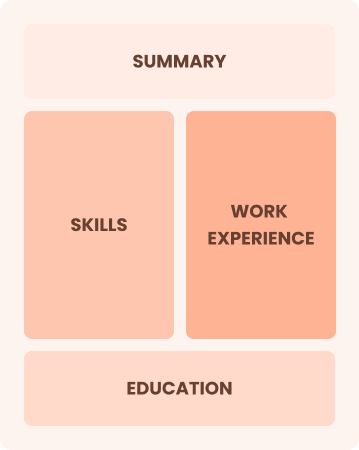
Resume Format Examples
Choosing the appropriate resume format is important for clearly showcasing your clinical research skills, relevant experience, and career advancements.
Entry-Level 0 - 2 years
Functional
Focuses on skills rather than previous jobs
Best for:
Recent graduates and career changers with up to two years of experience
Mid-Career 3 - 7 years
Combination
Balances skills and work history equally
Best for:
Mid-career professionals eager to highlight their skills and growth potential
Experienced 8+ years
Chronological
Emphasizes work history in reverse order
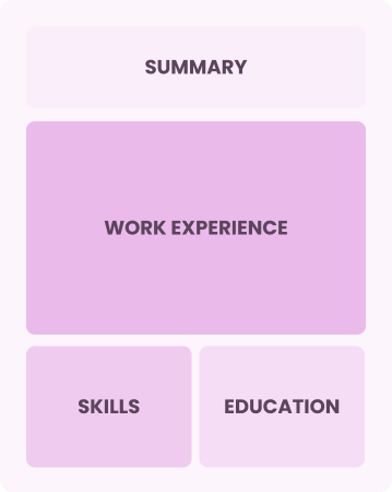
Best for:
Seasoned experts leading innovative clinical trials and research initiatives
Frequently Asked Questions
Should I include a cover letter with my clinical research associate resume?
Absolutely. Including a cover letter can significantly improve your application by showcasing your passion and relevant experience. It allows you to connect the dots between your skills and the job requirements. If you're looking for guidance, explore our resources on how to write a cover letter or use our Cover Letter Generator for quick assistance.
Can I use a resume if I’m applying internationally, or do I need a CV?
When applying for jobs outside the U.S., use a CV instead of a resume, as many countries prefer this format. To ensure your CV meets international standards, explore our comprehensive resources that provide CV examples and detailed guidance on how to write a CV.
What soft skills are important for clinical research associates?
Soft skills such as communication, critical thinking, and collaboration are essential for clinical research associates. These interpersonal skills foster strong relationships with team members and study participants, ensuring accurate data collection and a smooth research process.
I’m transitioning from another field. How should I highlight my experience?
Highlight your transferable skills like communication, analytical thinking, and project management acquired from previous roles. These abilities demonstrate your adaptability and potential contributions to clinical research. Offer concrete examples that align your past successes with the responsibilities of a clinical research associate, reinforcing your value even without extensive industry experience.
Where can I find inspiration for writing my cover letter as a clinical research associate?
For those pursuing clinical research associate positions, exploring professionally crafted cover letter examples can be invaluable. These samples not only provide inspiration for content ideas but also offer formatting tips and techniques to effectively showcase your qualifications. Use them as a guide to strengthen your application materials.
How do I add my resume to LinkedIn?
To add your resume to LinkedIn and improve its visibility, upload it to your profile or highlight key experiences in the "About" and "Experience" sections. This approach helps clinical research recruiters easily discover qualified applicants, increasing your chances of standing out in a competitive field.

Ready to land the job?
Join 28M+ others who've built a resume that works.