


Incorporating hard skills such as skill in circuit design, simulation tools, and understanding semiconductor physics is essential for creating effective analog systems.
Analog Design Engineer Resume Examples & Templates
Looking to stand out as an analog design engineer? Our analog design engineer resume examples will help you showcase your circuit design expertise and problem-solving skills that employers value.

by Gabriela Hernandez, Last Updated: January 18, 2026
Hired By:*

- Popular Analog Design Engineer Resume Examples
- Resume Template—Easy to Copy & Paste
- Build Your Resume in Minutes
- How to Write a Analog Design Engineer Resume Summary
- Showcasing Your Work Experience
- Top Skills to Include on Your Resume
- Resume Format Examples
- Related Engineering Resume Examples
- Frequently Asked Questions
- Should I include a cover letter with my analog design engineer resume?
- Can I use a resume if I’m applying internationally, or do I need a CV?
- What soft skills are important for analog design engineers?
- I’m transitioning from another field. How should I highlight my experience?
- Should I use a cover letter template?
- Should I include a personal mission statement on my analog design engineer resume?
Popular Analog Design Engineer Resume Examples
Check out our top analog design engineer resume examples that highlight key skills such as circuit design, problem-solving, and collaboration. These examples can help you effectively showcase your accomplishments to potential employers.
Are you looking to build your standout resume? The Resume Builder offers user-friendly templates specifically designed for engineers, making it simple to create a professional and effective presentation of your skills.
Recommended
 Customize This Resume
Entry-level analog design engineer resume
What this resume does well:
This entry-level resume for an analog design engineer highlights the applicant's design and optimization skills through concrete achievements, such as improving circuit performance and reducing development cycles. New professionals must clearly demonstrate their technical competencies and collaborative abilities to attract employers' attention, even with limited work history.
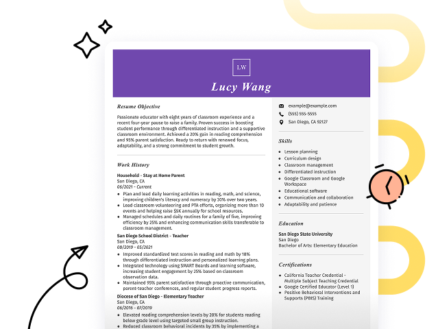
Mid-career analog design engineer resume
What this resume does well:
This resume effectively showcases the applicant's advanced qualifications in analog design, highlighting significant accomplishments and leadership experiences. The structured presentation of skills and responsibilities conveys readiness for greater challenges and positions them as a capable engineer prepared for future roles.
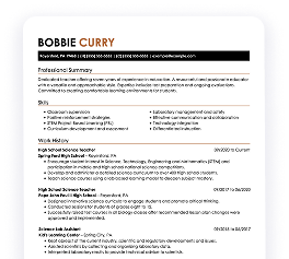
Experienced analog design engineer resume
What this resume does well:
This resume highlights the applicant’s extensive experience as an analog design engineer, showcasing significant achievements like a 30% efficiency improvement and $50K annual savings in power management. The clear formatting improves readability, making it easy for hiring managers to quickly recognize key contributions.
Resume Template—Easy to Copy & Paste
Example
Yuki Smith
Brookfield, WI 53017
(555)555-5555
Yuki.Smith@example.com
Skills
- Circuit Design
- Analog IC Design
- Mixed-Signal Design
- RF Circuitry
- PCB Layout
- Simulation Tools
- Power Optimization
- Team Leadership
Languages
- Spanish - Beginner (A1)
- French - Bilingual or Proficient (C2)
- German - Intermediate (B1)
Professional Summary
Innovative Analog Design Engineer with 5 years of industry experience, excelling in circuit design, mixed-signal development, and RF solutions to enhance efficiency. Proven leadership in engineering teams and significant contributions to project optimization.
Work History
Analog Design Engineer
MicroTech Electronics - Brookfield, WI
January 2023 - October 2025
- Designed circuits leading to 20% efficiency boost
- Reduced power consumption by 15% through optimization
- Led a team of 5 engineers on analog design projects
RF Circuit Designer
SignalIo Technologies - Milwaukee, WI
June 2021 - December 2022
- Developed RF circuits enhancing signal by 30%
- Collaborated with R&D to prototype new designs
- Managed component selection reducing costs by 10%
Mixed-Signal Design Engineer
Innovix Systems - Milwaukee, WI
January 2020 - May 2021
- Developed mixed-signal modules for consumer devices
- Improved system performance by 25% via integration
- Oversaw prototype validation ensuring project timelines
Certifications
- Certified Analog IC Designer - Institute of Electrical and Electronics Engineers (IEEE)
- Advanced RF Circuit Design - RF Design Certification Board
Education
Master of Science Electrical Engineering
Stanford University Stanford, California
May 2019
Bachelor of Science Electrical Engineering
University of Utah Salt Lake City, Utah
May 2017
Build Your Resume in Minutes
Creating a custom resume is easier than ever with our Resume Builder!
How to Write a Analog Design Engineer Resume Summary
Your resume summary is the first opportunity to make a lasting impression on employers. It should clearly demonstrate how your skills and experiences align with the needs of an analog design engineer.
As an analog design engineer, you want to highlight your technical skill in circuit design and your ability to solve complex problems. Focus on showcasing your relevant projects and achievements that reflect your expertise in this field.
To guide you in crafting an effective summary, consider these examples that illustrate effective strategies for presenting yourself as a standout applicant:
Weak Example
I am an analog design engineer with several years of experience in various projects. I am looking for a job where I can use my skills and help the company succeed. A position that offers stability and room for advancement would be perfect for me. I believe I could add value to any team if given the chance.
Why this summary misses the mark:
- Contains broad statements about experience without detailing specific skills or achievements
- Relies heavily on personal language, making it feel less professional and more self-serving
- Emphasizes what the job seeker desires from the job rather than highlighting contributions they can make to potential employers
Strong Example
Results-driven analog design engineer with over 7 years of experience in designing high-frequency RF circuits and optimizing signal integrity for consumer electronics. Spearheaded a project that improved circuit performance by 30%, resulting in a product launch ahead of schedule. Proficient in using tools such as Cadence, MATLAB, and SPICE for simulations and analysis.
Why this summary works:
- Begins with clear experience level and specific areas of expertise in analog design
- Highlights quantifiable achievement that illustrates significant improvement in performance metrics
- Mentions relevant technical skills and tools that are essential for the role, showcasing competency
Pro Tip
If you’re short on formal experience, consider using a career objective to highlight your passion and skills effectively. Check out various resume objective examples tailored to the analog design engineering field to inspire your own.
Showcasing Your Work Experience
The work experience section is important for your resume as an analog design engineer, and it will contain the bulk of your content. Good resume templates always emphasize this important area.
In this section, you should list your previous roles in reverse-chronological order, detailing your responsibilities and accomplishments. Use bullet points to succinctly highlight specific achievements in each position.
To help you better understand how to craft this section effectively, we’ll now present a couple of examples that illustrate what works well and what could be improved:
Weak Example
Analog Design Engineer
Tech Innovations Corp – San Jose, CA
- Designed circuits for various applications.
- Collaborated with team members on projects.
- Tested and validated designs in the lab.
- Assisted in troubleshooting issues with prototypes.
Why this work experience section misses the mark:
- Lacks specific employment dates to provide context
- Bullet points are vague and do not highlight key achievements
- Emphasizes routine tasks rather than effective contributions
Strong Example
Analog Design Engineer
Tech Innovations Inc. – San Jose, CA
March 2020 - Current
- Develop high-performance analog circuits for consumer electronics, improving power efficiency by 30%.
- Spearhead design reviews and testing processes that reduced time to market by 20%.
- Mentor junior engineers in best practices, fostering a collaborative environment that improves skill development.
Why this work experience section works:
- Uses effective action verbs to clearly demonstrate the engineer's contributions
- Incorporates specific metrics that showcase quantifiable achievements in performance
- Highlights mentorship and collaboration, essential skills for success in engineering roles
While your resume summary and work experience are important, don't overlook the importance of other sections. Each part plays a role in showcasing your qualifications. For more detailed guidance on crafting a standout resume, be sure to read our comprehensive guide on how to write a resume.
Top Skills to Include on Your Resume
A well-crafted skills section is key for any resume, as it succinctly showcases your qualifications to potential employers. This part lets hiring managers quickly assess if you have the necessary expertise for the role.
For an analog design engineer, it's important to highlight both technical skills and relevant tools. Focus on specific software like Cadence, Mentor Graphics, and circuit simulation tools that demonstrate your skill in designing analog circuits effectively.
Meanwhile, soft skills like problem-solving abilities, teamwork, and communication facilitate collaboration with cross-functional teams and ensure successful project outcomes.
When selecting skills for your resume, it’s essential to align them with what employers expect. Many companies use automated systems to filter out job seekers lacking the necessary resume skills, so making this match is important.
To improve your chances of being noticed, carefully read job postings for insights on which skills to emphasize. This approach not only attracts recruiters' attention but also helps ensure your application meets ATS requirements effectively.
Pro Tip
Ensure your resume stands out in the digital crowd. Use our ATS Resume Checker to catch over 30 common pitfalls that could hold you back from landing your dream role.
10 skills that appear on successful analog design engineer resumes
Make your resume stand out to recruiters by highlighting essential skills for analog design engineers. These sought-after qualifications can be seen in our resume examples, helping you apply with the assurance a polished resume provides.
Here are 10 skills you should consider including in your resume if they align with your experience and job requirements:
Circuit design
Signal processing
Analog circuit troubleshooting
Project management
Schematic capture
SPICE simulation skill
Component selection
PCB layout expertise
Testing and validation techniques
Collaboration with cross-functional teams
Based on analysis of 5,000+ engineering professional resumes from 2023-2024
Resume Format Examples
Choosing the right resume format is important for an analog design engineer because it effectively highlights your technical expertise, relevant experience, and professional growth in a clear and organized manner.
Entry-Level 0 - 2 years
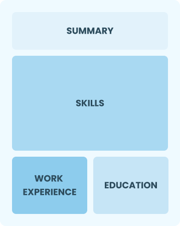
Functional
Focuses on skills rather than previous jobs
Best for:
Recent graduates and career changers with up to two years of experience
Mid-Career 3 - 7 years
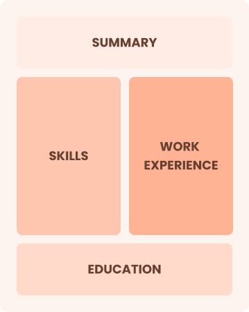
Combination
Balances skills and work history equally
Best for:
Mid-career professionals focused on demonstrating their skills and seeking growth opportunities
Experienced 8+ years
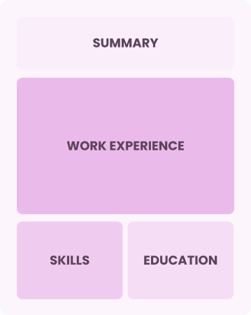
Chronological
Emphasizes work history in reverse order
Best for:
Senior nurses leading specialized care teams with expertise in patient management
Frequently Asked Questions
Should I include a cover letter with my analog design engineer resume?
Absolutely. Including a cover letter can greatly improve your application by showcasing your unique qualifications and enthusiasm for the position. It gives you the chance to elaborate on your experience beyond your resume. For tips on crafting an effective cover letter, explore our comprehensive guide on how to write a cover letter or use our Cover Letter Generator for a quick start.
Can I use a resume if I’m applying internationally, or do I need a CV?
When applying for jobs outside the U.S., use a CV instead of a resume, as many countries prefer this format. To create an effective CV, explore CV examples that showcase proper formatting and layouts. Additionally, learn more about how to write a CV to ensure your application meets international standards.
What soft skills are important for analog design engineers?
Soft skills like communication, problem-solving, and interpersonal skills are essential for analog design engineers. These skills foster effective teamwork, enabling engineers to share ideas, troubleshoot issues together, and create innovative solutions that meet project goals.
I’m transitioning from another field. How should I highlight my experience?
Highlight your transferable skills such as analytical thinking, project management, and teamwork when applying for analog design engineer roles. Demonstrating these abilities shows your value even if your background is in a different field. Use concrete examples from past projects to illustrate how your experiences align with the demands of analog design engineering.
Should I use a cover letter template?
Yes, using a cover letter template tailored for an analog design engineer ensures organized content that effectively highlights relevant skills such as circuit design skill and experience with simulation tools, making it easier for hiring managers to see your qualifications at a glance.
Should I include a personal mission statement on my analog design engineer resume?
Yes, including a personal mission statement on your resume is advisable. It helps convey your engineering values and aspirations effectively. This technique works particularly well when targeting companies that emphasize innovation, sustainability, or collaborative cultures by aligning your goals with their mission.

Ready to land the job?
Join 28M+ others who've built a resume that works.