


Hard skills are technical abilities such as skill in engineering software, understanding of structural analysis, and knowledge of materials science that are essential for effective project execution.
Engineer Resume Examples & Templates
Looking to boost your career as an engineer? Our engineer resume examples will help you showcase your technical skills and project management expertise to catch the eye of potential employers.

by Gabriela Hernandez, Last Updated: January 18, 2026
Hired By:*

- Popular Engineer Resume Examples
- Resume Template—Easy to Copy & Paste
- Build Your Resume in Minutes
- How to Write a Engineer Resume Summary
- Showcasing Your Work Experience
- Top Skills to Include on Your Resume
- Resume Format Examples
- Engineer Salaries in the Highest-Paid States
- Related Engineering Resume Examples
- Frequently Asked Questions
- Should I include a cover letter with my engineer resume?
- Can I use a resume if I’m applying internationally, or do I need a CV?
- What soft skills are important for engineers?
- I’m transitioning from another field. How should I highlight my experience?
- Should I use a cover letter template?
- Should I include a personal mission statement on my engineer resume?
Popular Engineer Resume Examples
Check out our top engineer resume examples that demonstrate key skills such as problem-solving, technical expertise, and project management. These examples will help you showcase your achievements effectively.
Want to build your own impressive resume? The Resume Builder offers user-friendly templates designed specifically for engineers, making the process straightforward and efficient.
Recommended
 Customize This Resume
Entry-level engineer resume
What this resume does well:
This entry-level resume for an engineering position effectively highlights the applicant's technical skills and significant accomplishments in previous roles, showcasing a strong foundation in mechanical engineering. New professionals in this field must demonstrate their ability to drive efficiency and innovation through quantifiable achievements, even if their work history is limited.
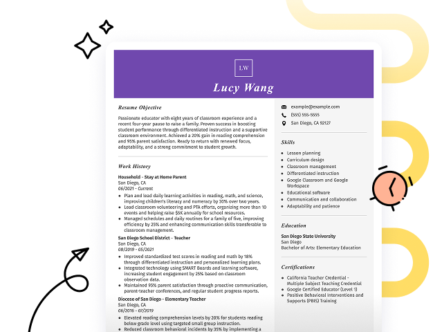
Mid-career engineer resume
What this resume does well:
This resume effectively showcases the applicant's qualifications by detailing compelling projects and leadership roles. The structured presentation highlights a progressive career trajectory, demonstrating readiness for advanced engineering challenges and responsibilities within dynamic environments.
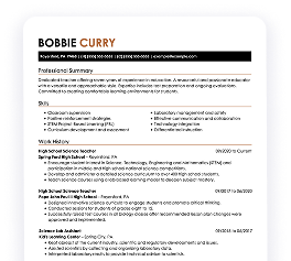
Experienced engineer resume
What this resume does well:
This resume demonstrates the applicant's strong engineering expertise, highlighting achievements such as increasing efficiency by 20% and saving $50k annually through system development. The clear formatting effectively showcases accomplishments, making it easy for hiring managers to assess qualifications quickly.
Resume Template—Easy to Copy & Paste
Example
John Chen
Tacoma, WA 98402
(555)555-5555
John.Chen@example.com
Skills
- Project Management
- Mechanical Design
- System Engineering
- Process Improvement
- Efficiency Optimization
- Team Leadership
- Budget Management
- Resource Allocation
Languages
- Spanish - Beginner (A1)
- German - Beginner (A1)
- Mandarin - Intermediate (B1)
Professional Summary
Seasoned engineer with expertise in project management and process optimization. Led teams to enhance efficiency with 15% improvements. Skilled in budget management and mechanical design.
Work History
Engineer
Tech Innovations Inc. - Tacoma, WA
November 2023 - October 2025
- Led team to increase efficiency by 15%
- Managed projects with budgets up to 0K
- Developed improved engineering processes
Development Engineer
NextGen Solutions - Eastside, WA
January 2021 - October 2023
- Reduced cost by 18% through new designs
- Supervised 12 junior engineers
- Enhanced system reliability by 10%
Assistant Engineer
Innovative Tech Works - Silverlake, WA
January 2020 - December 2020
- Drafted reports presenting 20% optimizations
- Supported remote team integration
- Facilitated 30% resource reallocation
Certifications
- Certified Professional Engineer - National Society of Professional Engineers
- Lean Six Sigma Green Belt - American Society for Quality
Education
Master of Science Mechanical Engineering
Stanford University Stanford, California
June 2019
Bachelor of Science Mechanical Engineering
University of California, Berkeley Berkeley, California
June 2018
Build Your Resume in Minutes
Creating a custom resume is easier than ever with our Resume Builder!
How to Write a Engineer Resume Summary
Your resume summary is the first opportunity to impress hiring managers, making it important to effectively showcase your qualifications. As an engineer, highlight your technical skills and project experience that demonstrate your ability to solve complex problems.
In this section, you should emphasize your achievements and the specific engineering disciplines you've mastered. This will set you apart from other job seekers and give employers a clear picture of what you bring to the table.
To guide you in crafting a compelling summary, review these examples that illustrate effective approaches and common pitfalls:
Weak Example
I am an experienced engineer looking for a job where I can use my skills and knowledge. My goal is to find a position that allows me to grow and succeed while contributing to the company's success. I believe I would be a great addition to your team if given the chance.
Why this summary misses the mark:
- Lacks specific details about engineering expertise or accomplishments, making it sound generic
- Emphasizes personal goals rather than showcasing what value the applicant brings to potential employers
- Uses vague language, such as 'experienced' without specifying areas of engineering or technical skills
Strong Example
Results-driven engineer with 7+ years of experience in mechanical design and development, specializing in product optimization and efficiency improvements. Led a project that increased production efficiency by 20%, saving the company $150,000 annually. Proficient in CAD software, lean manufacturing principles, and cross-functional teamwork to deliver innovative engineering solutions.
Why this summary works:
- Begins with a clear indication of experience level and technical expertise
- Highlights quantifiable results demonstrating impact on operational efficiency
- Mentions specific technical skills that are highly relevant to engineering roles
Pro Tip
If you're new to the workforce, consider using a career objective on your resume instead of a summary. This approach highlights your goals and enthusiasm. Check out various resume objective examples tailored for engineering roles to get inspired.
Showcasing Your Work Experience
The work experience section is the cornerstone of your resume as an engineer. This area will contain the bulk of your content, and resume templates always feature this important section prominently.
In this section, you'll list your previous positions in reverse-chronological order, detailing your roles and responsibilities. Bullet points are key here, allowing you to highlight specific achievements and contributions for each position.
To help guide you in crafting an effective work history, we've put together a couple of examples that illustrate what works well and what should be avoided:
Weak Example
Engineer
Global Tech Solutions – San Francisco, CA
- Designed projects for clients.
- Collaborated with team members.
- Reviewed technical documents.
- Assisted in meetings and discussions.
Why this work experience section misses the mark:
- Lacks specific details about the projects or technologies used
- Bullet points are overly general and do not highlight individual contributions
- Does not mention any measurable outcomes or successes achieved
Strong Example
Engineer
Tech Innovations Inc. – San Francisco, CA
March 2020 - Present
- Led the design and implementation of a new software system that increased data processing speed by 40%.
- Collaborated with cross-functional teams to reduce project delivery time by 30%, improving overall client satisfaction.
- Mentored junior engineers, fostering skill development and promoting a culture of continuous improvement.
Why this work experience section works:
- Starts each bullet with effective action verbs that showcase the job seeker’s achievements
- Incorporates quantifiable results to demonstrate effectiveness and impact on projects
- Highlights essential skills relevant to engineering while displaying leadership and teamwork capabilities
While your resume summary and work experience are critical components, don’t overlook the importance of other sections. Each part plays a role in presenting your qualifications effectively. For more detailed guidance, explore our comprehensive how to write a resume guide.
Top Skills to Include on Your Resume
A strong resume must include a technical skills section to effectively showcase your qualifications. This area allows employers to quickly identify if you possess the essential abilities for the engineering role.
As an engineer, highlight both technical skills and relevant tools. You should mention software like AutoCAD or MATLAB, as well as systems such as project management tools that demonstrate your expertise in the field.
Soft skills are interpersonal qualities like teamwork, problem-solving, and communication that foster collaboration and innovation within engineering projects.
Selecting the right resume skills is important for aligning with what employers expect from job seekers. Many organizations use automated systems to filter out applicants who lack the essential skills needed for the position.
To effectively showcase your qualifications, review job postings carefully to identify key skills that recruiters highlight. This strategy will help you tailor your resume, ensuring it resonates with both hiring managers and ATS systems alike.
Pro Tip
Increase your resume's impact by using our ATS Resume Checker, which identifies over 30 common errors and improves your chances of bypassing applicant tracking systems.
9 skills that appear on successful engineer resumes
Improving your resume with high-demand skills is key to attracting attention from recruiters in engineering roles. Integrating these sought-after skills can greatly boost your application, as shown in our resume examples, enabling you to pursue job opportunities confidently.
By the way, here are 9 essential skills that you should consider incorporating into your resume if they align with your expertise and job criteria:
Root-cause analysis
Time management
Product development
Process improvement
Project planning
Project management
Critical thinking
Technical reporting
Failure analysis
Based on analysis of 5,000+ engineering professional resumes from 2023-2024
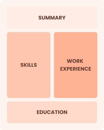
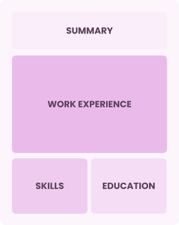
Resume Format Examples
Selecting the appropriate resume format is important for engineers, as it emphasizes key technical skills, relevant experience, and career advancement in a clear and organized manner.
Entry-Level 0 - 2 years
Functional
Focuses on skills rather than previous jobs
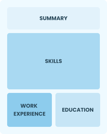
Best for:
Recent graduates and career changers with up to two years of experience
Mid-Career 3 - 7 years
Combination
Balances skills and work history equally
Best for:
Engineers seeking to demonstrate their skills and pursue new opportunities
Experienced 8+ years
Chronological
Emphasizes work history in reverse order
Best for:
Engineers leading innovative projects with extensive industry experience
Engineer Salaries in the Highest-Paid States
Our engineer salary data is based on figures from the U.S. Bureau of Labor Statistics (BLS), the authoritative source for employment trends and wage information nationwide.
Whether you're entering the workforce or considering a move to a new city or state, this data can help you gauge what fair compensation looks like for engineers in your desired area.
$0$210K$420K
Frequently Asked Questions
Should I include a cover letter with my engineer resume?
Absolutely, including a cover letter can significantly improve your application by showcasing your personality and clarifying your qualifications. It allows you to connect with recruiters on a personal level. For tips on crafting an impressive cover letter, consider our detailed guide on how to write a cover letter or use our Cover Letter Generator for quick assistance.
Can I use a resume if I’m applying internationally, or do I need a CV?
When applying for jobs abroad, use a CV instead of a resume. A CV provides a comprehensive overview of your academic and professional history, which is often preferred in many countries. Explore CV examples and learn how to write a CV to craft a compelling document that meets international standards.
What soft skills are important for engineers?
Soft skills like communication, problem-solving, and teamwork are essential for engineers. These interpersonal skills foster collaboration among team members and facilitate clear interaction with clients, leading to innovative solutions and successful project outcomes.
I’m transitioning from another field. How should I highlight my experience?
Highlight your transferable skills such as teamwork, communication, and analytical thinking when applying for engineering roles. These competencies are important in problem-solving and project execution, making you a valuable asset despite limited direct experience. Share concrete examples from previous positions to illustrate how your abilities align with the responsibilities of an engineer.
Should I use a cover letter template?
Yes, using a cover letter template tailored for engineering roles can improve your letter's structure and organization. This allows you to effectively showcase critical skills such as project management, technical skill, and problem-solving achievements that resonate with hiring managers.
Should I include a personal mission statement on my engineer resume?
Yes, including a personal mission statement on your resume is recommended. It effectively conveys your core values and career ambitions. This approach works particularly well when targeting organizations that prioritize innovation and teamwork, as it aligns with their culture and vision.

Ready to land the job?
Join 28M+ others who've built a resume that works.