Hard skills include expertise in semiconductor fabrication, circuit design, and materials science, all essential for developing advanced technologies.
Advanced Semiconductor Engineer Resume Examples & Templates
Looking to elevate your career? Our advanced semiconductor engineer resume examples showcase essential skills like design expertise and problem-solving that will help you stand out to potential employers.

by Gabriela Hernandez, Last Updated: January 18, 2026
Hired By:*

Popular Advanced Semiconductor Engineer Resume Examples
Check out our top advanced semiconductor engineer resume examples that emphasize important skills such as circuit design, system optimization, and project management. These examples will help you showcase your technical expertise effectively.
Looking to build your own resume? Our Resume Builder offers user-friendly templates designed specifically for engineers, making it simple to create a professional and strong document.
Recommended
 Customize This Resume
Entry-level advanced semiconductor engineer resume
What this resume does well:
This entry-level resume for an Advanced Semiconductor Engineer effectively showcases the job seeker's technical expertise and innovative contributions, such as patenting a novel IC design. New professionals in this field must demonstrate their ability to apply theoretical knowledge through practical achievements and collaborative project experiences, even with limited work history.
Mid-career advanced semiconductor engineer resume
What this resume does well:
This resume effectively showcases the job seeker's extensive experience and achievements in semiconductor engineering. The clear presentation of leadership roles and quantifiable successes reflects their readiness to tackle complex challenges and assume greater responsibilities in advanced positions.
Experienced advanced semiconductor engineer resume
What this resume does well:
This resume illustrates the applicant's extensive experience as an advanced semiconductor engineer, highlighting significant achievements like improving yield rates by 25% and reducing production downtime by 30%. The bullet-point format effectively improves readability, making it ideal for hiring managers seeking specific accomplishments.
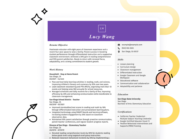
Resume Template—Easy to Copy & Paste
Example
Chris Wang
San Diego, CA 92107
(555)555-5555
Chris.Wang@example.com
Skills
- Semiconductor manufacturing
- Lithography and process optimization
- Advanced material engineering
- Cleanroom protocols and analysis
- Microfabrication techniques
- Simulation modeling software (COMSOL, Cadence)
- Thermal and optical testing solutions
- Failure analysis and remediation
Languages
- Mandarin Chinese - Beginner (A1)
- German - Beginner (A1)
- Japanese - Intermediate (B1)
Professional Summary
Expert Semiconductor Engineer with 9 years of experience in microfabrication, advanced lithography, and cleanroom process optimization. Proven ability to design and improve chips, reduce defect rates, and streamline manufacturing efficiencies. Highly skilled in emerging material solutions and leading semiconductor innovation.
Work History
Advanced Semiconductor Engineer
Quantum Micro Systems - San Diego, CA
February 2022 - September 2025
- Designed 5nm node prototypes, reducing defect rate by 25%
- Optimized lithography process, cutting cycle time by 15%
- Improved cleanroom efficiency, upgrading output by 20% annually
Semiconductor Process Engineer
Nano Circuit Manufacturing - Lakeside, CA
March 2017 - January 2022
- Refined etching tools, boosting etch accuracy by 18%
- Conducted thermal analysis, reducing energy cost by K
- Led installation of automated systems, saving 10% downtime
Microfabrication Design Engineer
Precision Silica Labs - Lakeside, CA
February 2014 - February 2017
- Improved wafer quality KPI by 28% through material research
- Developed advanced simulation models, shortening R&D by 22%
- Audited line processes, saving K annually on material waste
Certifications
- Certified Semiconductor Process Engineer (CSPE) - Institute of Electrical and Electronics Engineers (IEEE)
- Advanced Lithography Certification - Semiconductor Industry Association
- Cleanroom Management Certification - International Society for Microelectronics
Education
Master of Science Electrical Engineering
Stanford University Stanford, California
May 2014
Bachelor of Science Materials Science
University of California, Berkeley Berkeley, California
May 2012
Build Your Resume in Minutes
Creating a custom resume is easier than ever with our Resume Builder!
How to Write a Advanced Semiconductor Engineer Resume Summary
Your resume summary is the first thing employers will see, making it essential to craft a strong introduction that showcases your qualifications. As an advanced semiconductor engineer, you should highlight your technical expertise and innovative problem-solving skills relevant to the field.
This profession demands a focus on achievements in design, development, and production processes within semiconductor technology. Emphasizing your experience with cutting-edge tools and methodologies will set you apart.
To illustrate what makes a compelling resume summary, consider the following examples that will clarify effective strategies for this critical section:
Weak Example
I am an advanced semiconductor engineer with years of experience in the industry. I seek a position where I can use my skills and help the company succeed. I would love to work in a place that values innovation and offers career development opportunities. I believe I can contribute positively to your team.
Why this summary misses the mark:
- Lacks specific examples of skills or achievements, making it vague
- Overly focused on personal desires instead of showcasing what value the job seeker brings to potential employers
- Uses generic phrases that do not differentiate the applicant from others in the field
Strong Example
Results-driven advanced semiconductor engineer with over 7 years of experience in designing and manufacturing cutting-edge semiconductor devices. Successfully led a project that improved yield rates by 20%, significantly improving production efficiency. Proficient in CAD tools, process simulation, and adhering to strict industry standards, which ensures high-quality deliverables.
Why this summary works:
- Highlights specific years of experience and relevant engineering expertise
- Includes quantifiable achievements that showcase a direct impact on production metrics
- Cites relevant technical skills essential for the role, positioning the job seeker as a strong fit for employers
Pro Tip
If formal work experience feels out of reach, consider crafting a compelling career objective. This approach can effectively highlight your aspirations and skills. Check out various resume objective examples specifically designed for advanced semiconductor engineering to guide you.
Showcasing Your Work Experience
The work experience section is the cornerstone of your resume as an advanced semiconductor engineer. This is where you will provide most of your information, and high-quality resume templates always feature this important section prominently.
Organize this part in reverse-chronological order to highlight your previous roles effectively. Use bullet points to succinctly convey your achievements and specific contributions in each engineering position.
To help you understand what makes a strong work history, we’ve compiled a couple of examples. These will showcase both effective strategies and common pitfalls to avoid when crafting your resume:
Weak Example
Advanced Semiconductor Engineer
Tech Innovations Inc. – San Jose, CA
- Designed semiconductor devices.
- Collaborated with team members.
- Conducted tests and reported results.
- Assisted in troubleshooting issues.
Why this work experience section misses the mark:
- Lacks specific employment dates to provide context
- Bullet points are too vague and do not highlight unique skills or accomplishments
- Focuses on basic responsibilities instead of strong contributions or results
Strong Example
Advanced Semiconductor Engineer
Tech Innovations Corp – San Jose, CA
March 2020 - Current
- Develop cutting-edge semiconductor designs that improved energy efficiency by 30% in high-performance applications.
- Lead a team of engineers in the successful rollout of a new fabrication process, reducing production costs by 15%.
- Collaborate with cross-functional teams to improve product testing protocols, achieving a 40% reduction in time-to-market for new products.
Why this work experience section works:
- Starts each bullet with strong action verbs to convey the job seeker’s contributions clearly
- Incorporates specific metrics that highlight tangible results and improvements achieved
- Showcases relevant engineering skills and collaboration efforts vital for success in the semiconductor field
While your resume summary and work experience are important components, don't overlook the importance of other sections that can improve your overall presentation. For more detailed guidance on crafting a standout resume, be sure to explore our comprehensive guide on how to write a resume.
Top Skills to Include on Your Resume
A skills section is essential for any resume because it lets you showcase your qualifications at a glance. This helps potential employers quickly identify if you have the necessary abilities for the advanced semiconductor engineer role.
For this position, highlight technical skills such as semiconductor fabrication techniques, knowledge of CAD software like AutoCAD, and skill with simulation tools such as SPICE. These specific skills demonstrate your expertise and readiness for the challenges ahead.
Soft skills such as problem-solving, teamwork, and communication abilities are important for collaborating effectively with multidisciplinary teams and driving innovation in the semiconductor industry.
Selecting the right resume skills is important for aligning with what employers expect from job seekers. Many organizations use automated screening tools that filter out applicants lacking essential qualifications for the job.
To improve your chances, review job postings carefully to identify key skills sought by recruiters and ATS systems. Highlighting these specific abilities in your resume will improve your visibility and appeal as a strong job seeker.
Pro Tip
Ensure your resume stands out by using our ATS Resume Checker, which highlights over 30 common pitfalls to help you craft a document that navigates applicant tracking systems smoothly and lands you that interview.
10 skills that appear on successful advanced semiconductor engineer resumes
Improve your resume to capture recruiters' attention by emphasizing key skills in high demand for advanced semiconductor engineers. Our resume examples showcase these essential skills, helping you apply with the assurance a polished resume provides.
Here are 10 skills you might consider adding to your resume if they align with your background and role expectations:
Circuit design
Signal integrity analysis
Device fabrication techniques
Semiconductor physics
Process optimization
Project management
Troubleshooting and debugging
Data analysis tools
Collaboration and teamwork
Technical documentation
Based on analysis of 5,000+ engineering professional resumes from 2023-2024
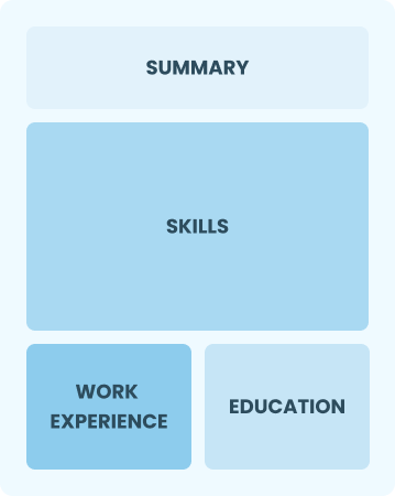
Resume Format Examples
Selecting the appropriate resume format is important for an advanced semiconductor engineer, as it highlights key technical skills, relevant experience, and career advancements effectively.
Entry-Level 0 - 2 years
Functional
Focuses on skills rather than previous jobs
Best for:
Recent graduates and career changers with up to two years of experience
Mid-Career 3 - 7 years
Combination
Balances skills and work history equally
Best for:
Mid-career professionals eager to demonstrate their skills and seek new challenges
Experienced 8+ years
Chronological
Emphasizes work history in reverse order
Best for:
Engineers excelling in cutting-edge technology and project leadership
Frequently Asked Questions
Should I include a cover letter with my advanced semiconductor engineer resume?
Absolutely, including a cover letter is a great way to improve your application and showcase your qualifications. A well-crafted cover letter allows you to highlight relevant experiences and demonstrate your enthusiasm for the position. If you're looking for tips on how to write a cover letter, check out our comprehensive guide or use our Cover Letter Generator for quick assistance.
Can I use a resume if I’m applying internationally, or do I need a CV?
When applying for jobs abroad, use a CV instead of a resume if the employer specifies it or if you're in fields like academia or research. Explore our resources for CV examples and how to write a CV for tips on formatting to create a compelling document that meets international expectations.
What soft skills are important for advanced semiconductor engineers?
Soft skills such as communication, problem-solving, and teamwork are essential for advanced semiconductor engineers. These interpersonal skills help foster collaboration with colleagues and encourage clear discussions with clients, ultimately driving innovation and success in complex projects.
I’m transitioning from another field. How should I highlight my experience?
When applying for advanced semiconductor engineer roles, highlight your transferable skills such as analytical thinking, teamwork, and project management. These abilities illustrate your capacity to tackle complex challenges and collaborate effectively, even if your background isn't in semiconductors. Use specific achievements from past experiences to showcase how you can add value to engineering projects.
Should I include a personal mission statement on my advanced semiconductor engineer resume?
Yes, including a personal mission statement in your resume is advisable. Highlighting your technical values and career aspirations through this statement can be especially strong when appealing to companies that emphasize innovation and sustainable practices in their culture.
How do I add my resume to LinkedIn?
To increase your resume's visibility on LinkedIn, you can add your resume to LinkedIn by uploading it directly to your profile or highlighting key achievements in the "About" and "Experience" sections. This strategy helps recruiters and hiring managers easily find qualified advanced semiconductor engineers like you, boosting your chances of connecting with potential job opportunities.

Ready to land the job?
Join 28M+ others who've built a resume that works.