


Hard skills are technical, measurable abilities such as data analysis, laboratory techniques, and research methodologies that a graduate research assistant must master.
Graduate Research Assistant Resume Examples & Templates
Ready to advance your academic career? Our graduate research assistant resume examples will help you showcase research skills and analytical abilities that catch the eye of hiring committees.

by Gabriela Hernandez, Last Updated: January 18, 2026
Hired By:*

- Popular Graduate Research Assistant Resume Examples
- Resume Template—Easy to Copy & Paste
- Build Your Resume in Minutes
- How to Write a Graduate Research Assistant Resume Summary
- Showcasing Your Work Experience
- Top Skills to Include on Your Resume
- Resume Format Examples
- Related Education Resume Examples
- Frequently Asked Questions
- Should I include a cover letter with my graduate research assistant resume?
- Can I use a resume if I’m applying internationally, or do I need a CV?
- What soft skills are important for graduate research assistants?
- I’m transitioning from another field. How should I highlight my experience?
- Where can I find inspiration for writing my cover letter as a graduate research assistant?
- Should I use a cover letter template?
Popular Graduate Research Assistant Resume Examples
Discover our top graduate research assistant resume examples that emphasize key skills such as data analysis, project management, and effective communication. These examples will help you effectively highlight your academic achievements and research contributions.
Ready to build a compelling resume? Our Resume Builder offers user-friendly templates specifically designed for aspiring researchers, making it simple to showcase your qualifications.
Recommended
 Customize This Resume
Entry-level graduate research assistant resume
What this resume does well:
This entry-level resume effectively highlights the applicant's substantial laboratory experience and contributions to research projects, showcasing skills in data analysis and project management. New professionals must clearly convey their technical competencies and collaborative experiences, ensuring that employers recognize their potential despite limited professional history.
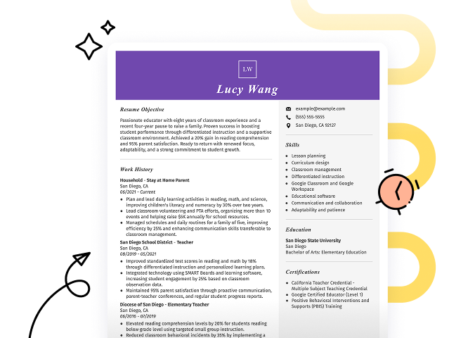
Mid-career graduate research assistant resume
What this resume does well:
This resume effectively showcases the applicant's qualifications by emphasizing powerful research contributions and technical expertise. The structured presentation of achievements and skills illustrates readiness for advanced roles, highlighting a solid trajectory in machine learning and data analysis.
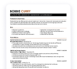
Experienced graduate research assistant resume
What this resume does well:
This resume's work history section illustrates the applicant's strong analytical skills and research capabilities, highlighted by preparing five research papers for publication and implementing machine learning models with 85% accuracy. The bullet-point format improves readability, making it easy for hiring managers to identify key achievements quickly.
Resume Template—Easy to Copy & Paste
Example
Olivia Rodriguez
Jacksonville, FL 32209
(555)555-5555
Olivia.Rodriguez@example.com
Professional Summary
Dynamic Graduate Research Assistant with 5 years in data analysis. Skilled in machine learning, statistical modeling, and project management. Published researcher recognized for innovation and academic excellence.
Work History
Graduate Research Assistant
AI Research Innovations - Jacksonville, FL
January 2023 - October 2025
- Developed algorithms improving efficiency by 20%
- Collaborated on projects boosting client satisfaction by 15%
- Analyzed datasets leading to 10% error reduction
Data Analysis Intern
Techno Data Solutions - Riverview, FL
January 2021 - December 2022
- Processed data improving accuracy by 30%
- Assisted in dashboard setup reducing report time by 25%
- Conducted market research enhancing strategy by 10%
Research Assistant Intern
Innovative Labs - Miami, FL
January 2020 - December 2020
- Supported breakthroughs increasing output by 15%
- Managed data collection improving efficiency by 12%
- Co-organized workshops increasing participation by 5%
Skills
- Data Analysis
- Machine Learning
- Statistical Modeling
- Python Programming
- Project Management
- Advanced Excel
- Research Methodologies
- Technical Writing
Education
Master of Science Computer Science
Boston University Boston, Massachusetts
June 2019
Bachelor of Science Data Science
University of Massachusetts Amherst, Massachusetts
June 2018
Certifications
- Certified Data Scientist - Data Science Council
- Advanced Python Programmer - Python Institute
Languages
- Spanish - Beginner (A1)
- French - Intermediate (B1)
- German - Beginner (A1)
Build Your Resume in Minutes
Creating a custom resume is easier than ever with our Resume Builder!
How to Write a Graduate Research Assistant Resume Summary
Your resume summary is the first thing employers will see, making it essential to create a compelling introduction that captures their attention. As a graduate research assistant, you should emphasize your analytical skills and relevant experience to demonstrate your capability in supporting research projects.
Highlighting your skill in data analysis, laboratory techniques, and collaboration with faculty or peers will set you apart from other job seekers. These elements are important in showcasing your qualifications for this role.
To illustrate effective strategies for crafting your summary, here are some examples that highlight what works well and what doesn’t:
Weak Example
I am a graduate research assistant with experience in various research projects. I am seeking a position where I can use my skills and contribute to innovative research. A supportive environment that encourages learning and collaboration is what I desire. I believe I would be a great addition to your team.
Why this summary misses the mark:
- Lacks specificity about the applicant’s skills and contributions to previous projects
- Overuses personal pronouns, which detracts from professionalism
- Emphasizes personal desires rather than highlighting how the applicant can add value to the employer
Strong Example
Motivated graduate research assistant with 3 years of experience in behavioral neuroscience, adept at designing and conducting experiments to investigate neural mechanisms of behavior. Contributed to a published study that increased understanding of anxiety disorders, leading to a 20% improvement in research efficiency through innovative data analysis techniques. Proficient in statistical software (SPSS, R) and laboratory techniques such as PCR and electrophysiology.
Why this summary works:
- Starts with clear experience level and specific field of expertise
- Highlights a quantifiable achievement that shows direct contribution to compelling research
- Mentions relevant technical skills that align with the requirements of research roles
Pro Tip
If formal work experience isn't your strong suit, consider crafting a career objective. This approach can effectively highlight your goals and aspirations. Check out various resume objective examples tailored specifically for graduate research roles to give you a head start.
Showcasing Your Work Experience
The work experience section is an important part of your resume as a graduate research assistant. This is where you’ll showcase the bulk of your content, and well-designed resume templates prioritize this section.
Organize this area in reverse-chronological order, highlighting your previous roles. Use bullet points to clearly detail your achievements and contributions in each position.
To illustrate what makes a powerful work history, we will present some examples that demonstrate effective practices and common pitfalls:
Weak Example
Graduate Research Assistant
University of Texas – Austin, TX
- Assisted in research projects
- Conducted experiments and collected data
- Collaborated with faculty members
- Wrote reports and presented findings
Why this work experience section misses the mark:
- Lacks specific employment dates for context
- Bullet points are vague and do not highlight unique contributions
- Emphasizes routine tasks rather than strong results or skills
Strong Example
Graduate Research Assistant
University of Madison – Madison, WI
August 2021 - Present
- Conduct detailed experiments in the field of microbiology, leading to a 30% increase in data accuracy for ongoing projects
- Collaborate with faculty and fellow researchers on grant proposals, securing over $50,000 in funding for innovative research initiatives
- Mentor undergraduate students in laboratory techniques, improving their practical skills and fostering a collaborative research environment
Why this work experience section works:
- Uses strong action verbs that clearly communicate the applicant's achievements
- Incorporates specific metrics that highlight tangible results and contributions
- Demonstrates relevant skills necessary for the role while showcasing teamwork and mentorship
While your resume summary and work experience are important components, don’t overlook the importance of other sections that contribute to a well-rounded presentation. For detailed guidance on crafting each part of your resume, be sure to explore our comprehensive guide on how to write a resume.
Top Skills to Include on Your Resume
A well-defined technical skills section is important for a standout resume, as it allows you to showcase your qualifications at a glance. This becomes even more important in competitive fields where employers quickly scan resumes for essential competencies.
For a graduate research assistant, it's important to highlight both hard skills and soft skills to show the full range of your abilities. Hard skills that demonstrate your subject matter expertise are essential, but so are soft skills that showcase your efficiency and interpersonal abilities.
Soft skills, including critical thinking, communication, and teamwork, are essential for collaborating on research projects and effectively conveying findings to diverse audiences.
When selecting skills for your resume, it’s important to align them with what employers expect. Many organizations implement automated screening systems that filter out job seekers lacking essential resume skills.
To improve your chances of passing these screenings, carefully review job postings related to your field. These postings often provide valuable insights into the specific skills recruiters prioritize, allowing you to tailor your resume effectively.
Pro Tip
To ensure your resume stands out in applicant tracking systems, use our ATS Resume Checker to uncover more than 30 common errors, giving your application the best chance of success.
10 skills that appear on successful graduate research assistant resumes
Highlighting relevant skills on your resume can significantly attract recruiters looking for graduate research assistants. You can explore resume examples to see how these essential skills are presented, helping you approach job applications with increased confidence.
By the way, adding relevant skills from the following list can improve your resume and align it with job requirements:
Research methodology
Data analysis
Technical writing
Project management
Collaboration
Statistical software skills
Laboratory techniques
Critical thinking
Presentation skills
Time management
Based on analysis of 5,000+ education professional resumes from 2023-2024
Resume Format Examples
Choosing the resume format that best suits your needs is essential for a graduate research assistant, as it effectively highlights relevant research skills, academic achievements, and your professional journey in the field.
Entry-Level 0 - 2 years
Functional
Focuses on skills rather than previous jobs
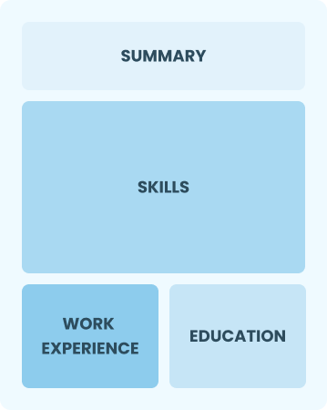
Best for:
Recent graduates and career changers with limited experience
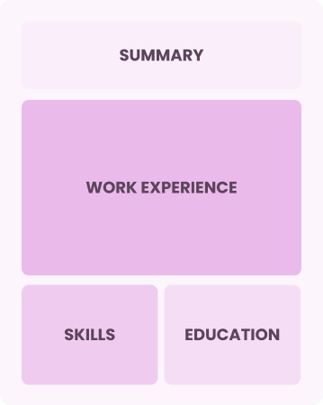
Mid-Career 3 - 7 years
Combination
Balances skills and work history equally
Best for:
Mid-career professionals eager to highlight their skills and growth potential
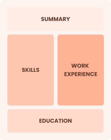
Experienced 8+ years
Chronological
Emphasizes work history in reverse order
Best for:
Experts leading innovative research projects and mentoring emerging scholars
Frequently Asked Questions
Should I include a cover letter with my graduate research assistant resume?
Absolutely, including a cover letter can significantly improve your application by allowing you to highlight your qualifications and demonstrate genuine interest in the position. If you're looking for guidance, we have an easy-to-follow guide on how to write a cover letter that can help you craft a compelling document. Alternatively, you can use our Cover Letter Generator for quick assistance.
Can I use a resume if I’m applying internationally, or do I need a CV?
When applying for jobs outside the U.S., use a CV instead of a resume, as it is often required for academic and research positions. To assist with formatting and writing your CV, explore our how to write a CV guide that walks you through global standards and best practices. For inspiration and structure, check out CV examples provided in our resources.
What soft skills are important for graduate research assistants?
Soft skills like communication, critical thinking, and collaboration are essential for graduate research assistants. These interpersonal skills foster effective teamwork with colleagues and help in clearly presenting research findings, ultimately leading to successful projects and a positive work environment.
I’m transitioning from another field. How should I highlight my experience?
Highlight your analytical, communication, and organizational skills gained from past roles. These transferable skills showcase your ability to thrive as a graduate research assistant. Use concrete examples to illustrate how you can apply past successes to research tasks, data management, and collaborative projects.
Where can I find inspiration for writing my cover letter as a graduate research assistant?
For those interested in graduate research assistant positions, exploring professionally crafted cover letter examples can be incredibly beneficial. These samples offer inspiration for content ideas, formatting tips, and effective methods to showcase your qualifications, ensuring your application stands out in a competitive field.
Should I use a cover letter template?
Using a cover letter template tailored for a graduate research assistant improves your ability to present structured content and showcase relevant research skills, such as data analysis and project management. By adopting this strategy, your academic achievements and technical expertise become effectively highlighted for hiring managers.

Ready to land the job?
Join 28M+ others who've built a resume that works.